-
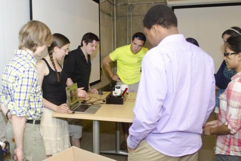 PEB students discuss the devices that they built in the Center for Engineering Innovation and Design during the 3D printing: design and fabrication Integrated Workshop module.
 -
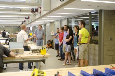 Touring the Center for Engineering Innovation and Design, where PEB students work on one of the Integrated Workshop lab modules.
 -
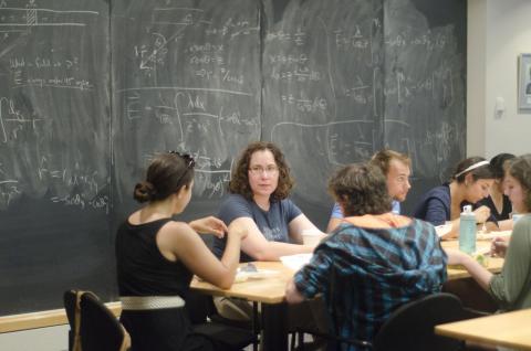 PEB students having lunch with Connecticut College undergraduates.
 -
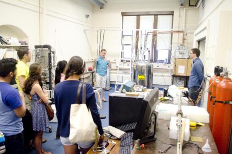 Tour of the Barrett lab and the NMRs.
 -
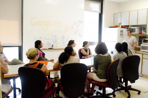 Undergrads hearing about what the Clark lab works on, prior to touring the lab and the fly setups.
 -
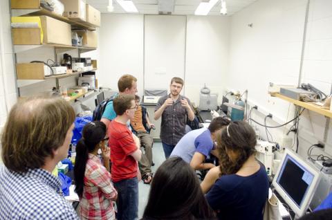 Getting to look at some samples under the microscope.
 -
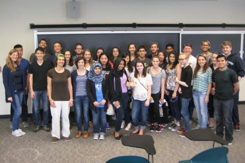 Connecticut College undergrads with PEB students and assistant director.
 -
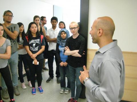 Hearing about what the Ganim lab works on prior to touring it.
 -
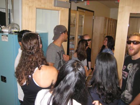 Putting on special safety glasses prior to seeing the optical setup in the Ganim lab.
 -
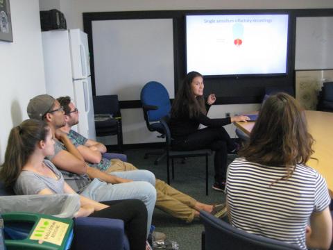 Short presentation prior to seeing the setup in the Carlson lab used to study how flies smell.
 -
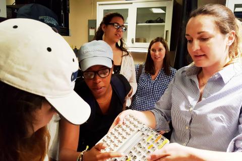 A Physics/PEB graduate student in the Malvankar lab showing AFM tips to Connecticut College undergraduates.
 -
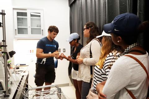 A MEMS/PEB student in the Howard lab showing Connecticut College students a microfluidics chamber..
 -
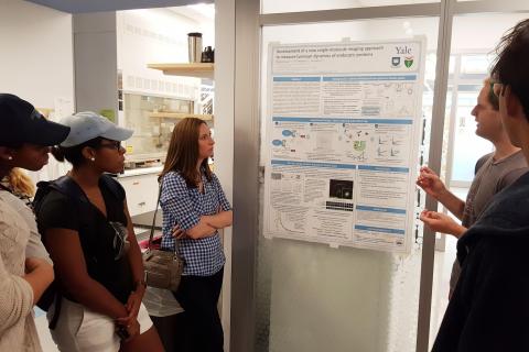 PEB students in the Berro lab explaining what they are working on in the lab.
August 4, 2015
This photo gallery depicts the annual visit of Connecticut College undergraduates to Yale.
